OPTICAL SILICONE MOLDING SOLUTIONS
Optical Silicone Lenses for High-Temperature LED & Sensor Applications
Custom transparent LSR optics engineered for UV resistance, anti-yellowing performance, and complex optical geometry. Direct DFM support from our tooling engineers.
Why Engineers Switch to Optical Silicone
When PC and PMMA optics begin to fail under heat, UV, and complex geometry demands, optical silicone becomes the engineering solution.
Engineering Capabilities at a Glance
| Capability | Specification |
|---|---|
| Optical Transmittance | ≥93% (typical, material dependent) |
| Operating Temperature | -60°C to +200°C continuous |
| Refractive Index | 1.40 – 1.43 |
| Hardness Range | Shore A 30 – 80 |
| Tooling Lead Time | T1 samples in 7–15 business days |
| Minimum Feature Size | Micro-optical textures supported |
| Supported File Types | STEP / STP / 2D PDF |
Typical Optical Silicone Applications
From LED secondary optics to automotive sensors, optical silicone solves engineering challenges where rigid plastics fall short.
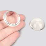
LED Secondary Optics
TIR optical silicone lenses, Fresnel structures, beam shapers, and light guides for high-power LED systems.
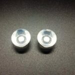
Automotive Lighting
DRL optics, adaptive headlight guides, and sensor optical windows requiring thermal cycling stability.
Sensor & Interface Optics
Optical coupling interfaces, transparent sensor covers, and light transmission windows.
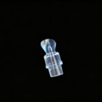
Medical & Beauty Optics
Light therapy optical components, medical optical assemblies, and transparent soft-touch interfaces.
Critical Manufacturing Risks in Optical Silicone Projects
Optical consistency during mass production is where most silicone optics projects fail. Here is how we engineer around each risk.
01
Bubble Entrapment Control
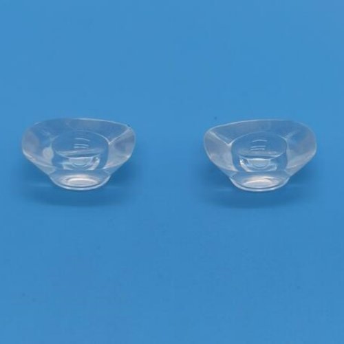
Microscopic trapped air in thick transparent sections creates beam inconsistency and optical clarity failures. We address this through vacuum material handling, controlled injection speed, and venting strategy optimization during DFM review.
Zero sampling. Every optical section verified.
02
Micro-Structure Replication
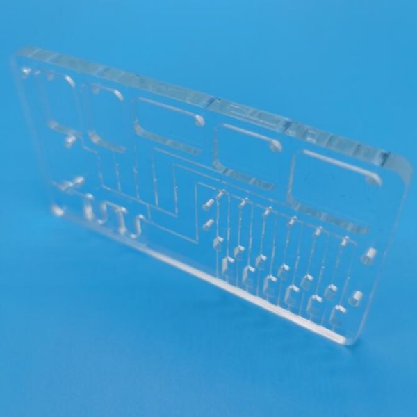
Optical textures like diffusion patterns, Fresnel structures, and beam shaping surfaces require highly stable tooling conditions. Our process controls mold temperature, venting balance, and low-viscosity flow to maintain replication consistency across production runs.
Tooling validated before mass production begins.
03
Flash Near Optical Surfaces
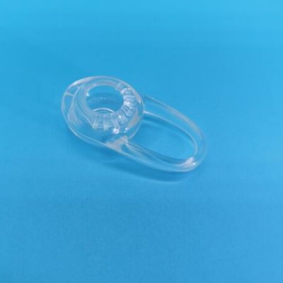
Even minor flash around optical edges creates light leakage and assembly instability. Precision mold fitting and controlled parting line positioning are evaluated during every DFM review to eliminate this risk before steel is cut.
Parting line strategy confirmed before tooling approval.
04
Thick-Wall Optical Distortion
Thick transparent geometries create sink marks, internal stress, and uneven transmission. Geometry DFM review, thickness balancing, and gate position optimization are applied to every thick-wall optical project.
Wall thickness reviewed at DFM stage, not after tooling.
Optical Silicone vs PC vs PMMA
Not every project needs optical silicone. Here is an honest comparison to help you decide.
| Property | Optical Silicone | PC | PMMA |
|---|---|---|---|
| UV Resistance | ✅ Excellent | ❌ Weak | ⚠️ Medium |
| Yellowing Resistance | ✅ Excellent | ❌ Weak | ⚠️ Medium |
| Heat Resistance | ✅ 150°C+ | ⚠️ ~120°C | ❌ ~90°C |
| Complex Geometry | ✅ Excellent | ⚠️ Medium | ⚠️ Medium |
| Flexible Integration | ✅ Excellent | ❌ Poor | ❌ Poor |
| Micro-Texture Replication | ✅ Excellent | ⚠️ Limited | ⚠️ Moderate |
When PC or PMMA remains the right choice: If your application operates at low temperature, stays indoors, uses simple flat geometry, and prioritizes lowest material cost — rigid plastics may remain the more economical solution. We will tell you this during DFM review if it applies to your project.
Frequently Asked Questions for Optical Silicone lenses
A1: Not always. Silicone delivers the most value for high-temperature, UV-exposed, outdoor, or geometrically complex optical applications. For simple indoor low-temperature geometry, PC or PMMA may remain more economical. We will advise you honestly during DFM review.
A2: Yes. Optical LSR materials replicate micro-optical tooling features with excellent consistency when tooling polish, mold temperature, and venting conditions are properly controlled and validated.
A3: The most common risks are trapped bubbles in thick sections, flash near optical surfaces, incomplete micro-feature filling, and optical distortion from wall thickness variation. All of these are evaluated during our DFM review before tooling begins.
A4: Prototype tooling typically delivers T1 samples within 7–15 business days after drawing approval. DFM feedback is provided within 1–3 days of receiving your STEP file.
A5: There is no fixed MOQ. We support projects from single-cavity prototype tooling through to high-volume production. Project scope is discussed during the DFM review based on your application and volume requirements.